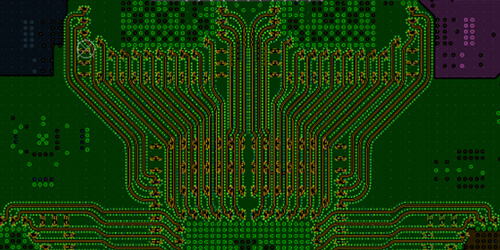
Before you can begin assembly of your printed circuit boards, you first need to get it through the PCB design and layout process. ACDi knows that getting an electronic device through production is hard work. We get it. We believe you deserve a true collaborator that will work with you through each phase of your project. For over 40 years, we’ve helped clients get over 11,000 projects from a CAD drawing to a real-world product.
Utilizing client specifications, ACDi provides layout and design services through the use of the latest tools and standards in the industry. In addition, ACDi’s PCB design team provides the added benefits from design for manufacturability (DFM), design for assembly (DFA), design for test (DFT) and design for cost (DFC) to further validate designs and prevent delays during production.
To get started with your PCB layout project, we will need the following documentation:
Our PCB designers take these key considerations and best practices into the PCB design process. They guide our PCB designers in creating PCBs that are optimized for production, testing, cost efficiency, and assembly. They help ensure the final product is not only functional but also practical and efficient to produce, meeting industry and business requirements.
Design for Manufacturability (DFM)
Design for Manufacturability (DFM) is the process of designing a PCB to ensure it can be manufactured efficiently and cost-effectively without errors or complications. DFM involves tailoring the design to align with the capabilities and limitations of fabrication and assembly processes. Key considerations include trace width and spacing, via types, panelization, and material selection. The goal is to minimize production risks, improve yield rates, and streamline the transition from design to production.
Design for Assembly (DFA)
Design for Assembly (DFA) emphasizes creating a PCB design that simplifies the assembly process. This includes standardizing component footprints, aligning component orientations, and ensuring adequate spacing for automated assembly tools. DFA also focuses on reducing manual assembly steps by eliminating awkward placements or orientations. By streamlining assembly, DFA minimizes production time, reduces errors, and lowers assembly costs.
Design for Test (DFT)
Design for Test (DFT) focuses on incorporating features into the PCB design that facilitate testing during and after manufacturing. This ensures that defects, such as open circuits, shorts, or faulty components, can be quickly identified and rectified. DFT often involves adding test points for automated testing equipment, ensuring accessible probe areas, and designing circuits with built-in self-tests (BIST). By enabling efficient testing, DFT reduces troubleshooting time, lowers repair costs, and improves product reliability.
Design for Cost (DFC)
Design for Cost (DFC) is the practice of optimizing the PCB design to reduce overall costs while maintaining performance and quality. This involves selecting cost-effective materials, minimizing the number of layers in a PCB, simplifying trace routing, and avoiding unnecessary design complexities. DFC also considers the long-term cost implications, such as repair, assembly, and component sourcing. Effective DFC strategies ensure that the product meets its cost targets without compromising on functionality or manufacturability.
By incorporating DFM, DFA, DFT and DFC principles into PCB design, engineers can create products that are efficient to manufacture, easy to test, cost-effective, and straightforward to assemble—ultimately leading to higher-quality and more reliable electronic devices.
For more information on our PCB layout and design capabilities, download the PDF.
Resources: